格物
有源像素传感器1966
active pixel sensor
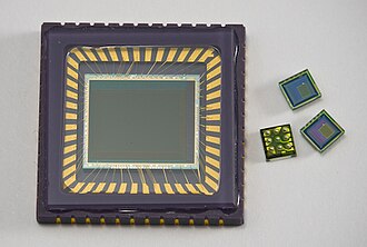
image sensor consisting of an integrated circuit
An active-pixel sensor (APS) is an image sensor where each pixel sensor unit cell has a photodetector and one or more active transistors. APS sensors are used in digital camera technologies such as cell phone cameras, web cameras, most modern digital pocket cameras, most digital single-lens reflex cameras (DSLRs), mirrorless interchangeable-lens cameras (MILCs), and lensless imaging for, e.g., blood cells.
摘自英文维基百科「Active-pixel sensor」(英文维基百科,暂无中文条目),CC BY-SA 4.0
- 类型
- 相机部件,特征与技术
- 发现 / 发明时间
- 1966 年
- 发现者 / 提出者
- Peter J W Noble
- 上级概念
- 图像传感器
- 组成部分
- 金属氧化物半导体场效应管、光度感应器、硅晶圆
- 用途
- 摄影、视频录制
百科正文
本条目暂无中文维基百科条目,下面是英文维基百科原文。
In a metal–oxide–semiconductor (MOS) active-pixel sensor, MOS field-effect transistors (MOSFETs) are used as amplifiers. There are different types of APS, including the early NMOS APS and the now much more common complementary MOS (CMOS) APS, also known as the CMOS sensor. CMOS sensors emerged as an alternative to charge-coupled device (CCD) image sensors and eventually outsold them by the mid-2000s.
The term active pixel sensor is also used to refer to the individual pixel sensor itself, as opposed to an array of such individuals, the image sensor. In this case, the image sensor is sometimes called an active pixel sensor imager or active-pixel image sensor.
History
Background
While researching metal–oxide–semiconductor (MOS) technology, Willard Boyle and George E. Smith discovered that an electric charge could be stored on a small MOS capacitor, which became the fundamental building block of the charge-coupled device (CCD) that they invented in 1969.
One of the main challenges with CCD technology was its reliance on nearly perfect charge transfer during readout. This limitation resulted in several drawbacks: relatively low radiation tolerance, poor performance in low-light conditions, manufacturing difficulties in producing large arrays, limited integration with on-chip electronics, reduced efficiency at low temperatures, constraints at high frame rates, and challenges in fabrication using non-silicon materials for extending wavelength response.
At RCA Laboratories, a research team including Paul K. Weimer, W.S. Pike and G. Sadasiv in 1969 proposed a solid-state image sensor with scanning circuits using thin-film transistors (TFTs), with photoconductive film used for the photodetector. A low-resolution "mostly digital" N-channel MOSFET (NMOS) imager with intra-pixel amplification, for an optical mouse application, was demonstrated by Richard F. Lyon in 1981. Another type of image sensor technology that is related to the APS is the hybrid infrared focal plane array (IRFPA), designed to operate at cryogenic temperatures in the infrared spectrum.
Comparison to CCDs
APS pixels solve the speed and scalability issues of the passive-pixel sensor. They generally consume less power than CCDs, have less image lag, and require less specialized manufacturing facilities. Unlike CCDs, APS sensors can combine the image sensor function and image processing functions within the same integrated circuit. APS sensors have found markets in many consumer applications, especially camera phones. They have also been used in other fields including digital radiography, military ultra high speed image acquisition, security cameras, and optical mice. Manufacturers include Aptina Imaging (independent spinout from Micron Technology, who purchased Photobit in 2001), Canon, Samsung, STMicroelectronics, Toshiba, OmniVision Technologies, Sony, and Foveon, among others. CMOS-type APS sensors are typically suited to applications in which packaging, power management, and on-chip processing are important. CMOS type sensors are widely used, from high-end digital photography down to mobile-phone cameras.
Advantages of CMOS compared with CCD
A primary advantage of a CMOS sensor is that it is typically less expensive to produce than a CCD sensor, as the image capturing and image sensing elements can be combined onto the same IC, with simpler construction required.
A CMOS sensor also typically has better control of blooming (that is, of bleeding of photo-charge from an over-exposed pixel into other nearby pixels).
Architecture
Pixel
The standard CMOS APS pixel consists of a photodetector (pinned photodiode), a floating diffusion, and the so-called 4T cell consisting of four CMOS (complementary metal–oxide–semiconductor) transistors, including a transfer gate, reset gate, selection gate and source-follower readout transistor. The pinned photodiode was originally used in interline transfer CCDs due to its low dark current and good blue response, and when coupled with the transfer gate, allows complete charge transfer from the pinned photodiode to the floating diffusion (which is further connected to the gate of the read-out transistor) eliminating lag. The use of intrapixel charge transfer can offer lower noise by enabling the use of correlated double sampling (CDS). The Noble 3T pixel is still sometimes used since the fabrication requirements are less complex. The 3T pixel comprises the same elements as the 4T pixel except the transfer gate and the photodiode. The reset transistor, Mrst, acts as a switch to reset the floating diffusion to VRST, which in this case is represented as the gate of the Msf transistor. When the reset transistor is turned on, the photodiode is effectively connected to the power supply, VRST, clearing all integrated charge. Since the reset transistor is n-type, the pixel operates in soft reset.
Design variants
Many different pixel designs have been proposed and fabricated. The standard pixel uses the fewest wires and the fewest, most tightly packed transistors possible for an active pixel. It is important that the active circuitry in a pixel take up as little space as possible to allow more room for the photodetector. High transistor count hurts fill factor, that is, the percentage of the pixel area that is sensitive to light. Pixel size can be traded for desirable qualities such as noise reduction or reduced image lag. Noise is a measure of the accuracy with which the incident light can be measured. Lag occurs when traces of a previous frame remain in future frames, i.e. the pixel is not fully reset. The voltage noise variance in a soft-reset (gate-voltage regulated) pixel is Vₙ²=kT/2C, but image lag and fixed pattern noise may be problematic. In rms electrons, the noise is (公式略).
Hard reset The pixel via hard reset results in a Johnson–Nyquist noise on the photodiode of Vₙ²=kT/C (公式略), but prevents image lag, sometimes a desirable tradeoff. One way to use hard reset is replace Mrst with a p-type transistor and invert the polarity of the RST signal. The presence of the p-type device reduces fill factor, as extra space is required between p- and n-devices; it also removes the possibility of using the reset transistor as an overflow anti-blooming drain, which is a commonly exploited benefit of the n-type reset FET.
以上节选摘自英文维基百科「Active-pixel sensor」,按 CC BY-SA 4.0 使用,去掉了参考文献、外部链接等尾部小节,公式改写成了纯文本。篇幅所限,较长的小节只摘了开头一部分,有的小节没有收;全文、配图和出处见原文。